

Memory Device and Method for Its Operation
| Publication Number: | GB2579058A |
| Application Date: | 16. 11. 2018 |
| Assignee/Applicant: | Jožef Stefan Institute [SI], Center of Excellence on Nanoscience and Nanotechnology [SI] |
| Inventor: | Anže Mraz, Damjan Svetin, Dragan Mihailović, Rok Venturini |
| Title: | Memory Device and Method for Its Operation |
| Description: | The invention presents a memory device (and method of use) whereby a switchable resistive element 4 and a superconductor element 3 are connected electrically in parallel (and preferably disposed in parallel in a stack). The switchable resistive element comprises active material, switchable between first and second electrical resistivity (p1, p2) values at the same temperature, (p1 different to p2). The active material may be 1T-TaS2, a layered dichalcogenide, chalcogenide or oxide material, and demonstrate resistive switching, charge density wave (CDW ordering), memristor or memory resistor behaviour. The superconductor element is operable such that part or all of the superconductor element is switch- able from a superconducting state to a non-superconducting state, and when this occurs a current injection passes through switchable resistive element capable of switching the switchable resistive element between first and second electrical resistivity values, representing first and second memory states. The memory device may be volatile or non-volatile. The superconductor may be a narrow channel or nanowire and include a constriction region to switch to a non superconducting state in preference to the reminder of the superconductor element. The device may be a two or three terminal device and current injection may be provided in a pulsed mode or continuous mode by an external circuit to activate the switch. Alternatively part of the superconductive element may be switched from superconducting to non-superconducting state by temperature. |
| Drawings: | 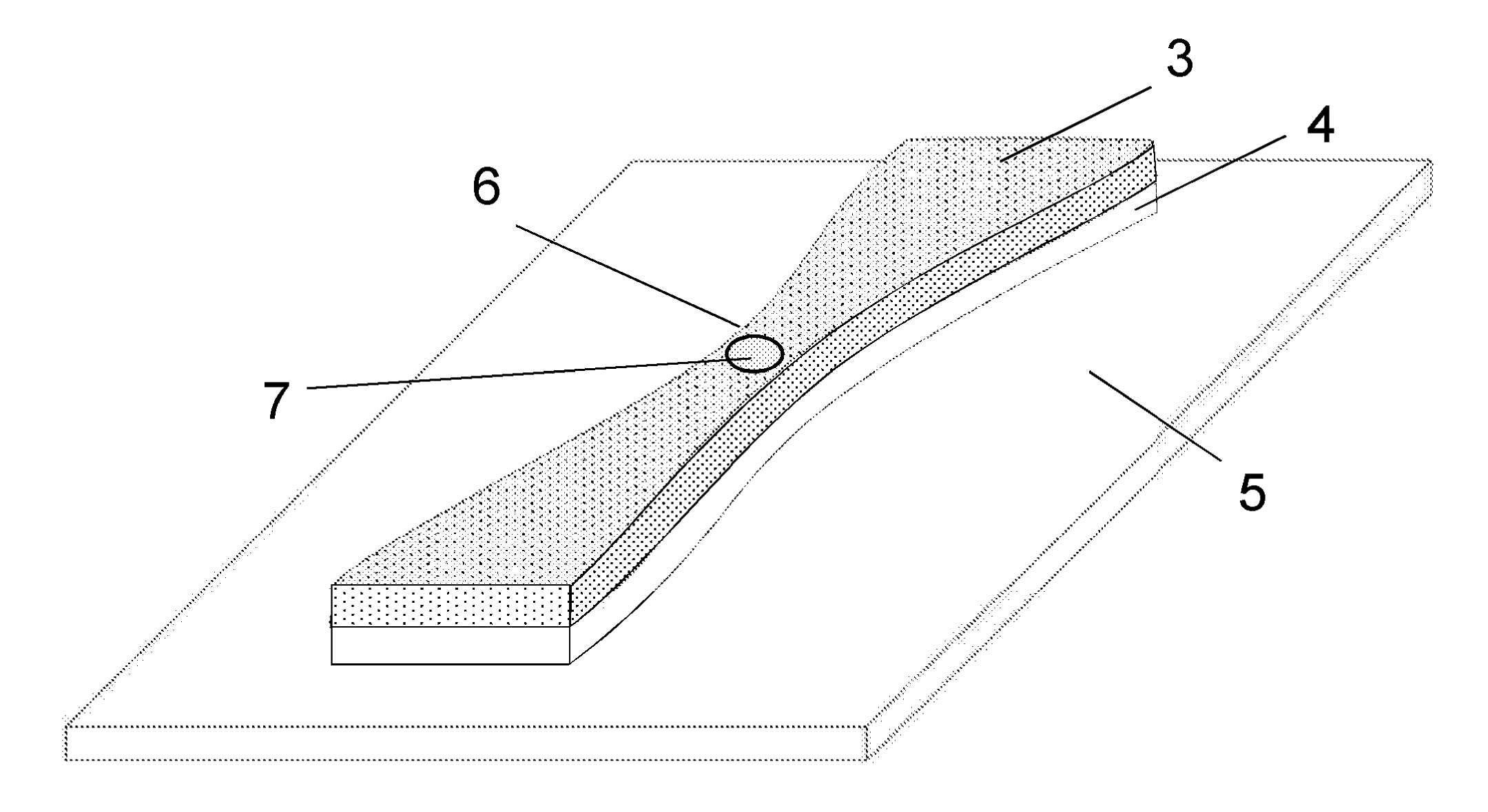 |
| Category: | Physical Sciences |
| Technology application codes: | Electronics, IT and telecoms |
| Market application codes: | Computer related, Other electronics related |
| www: | https://worldwide.espacenet.com/patent/search/family/064740161/publication/GB2579058A?q=svetin%20mraz%20venturini |
| Patent offices: | GB |
Extended patent application
| Publication Number: | WO2020099584A1 |
| Application Date: | 14. 11. 2019 |
| Assignee/Applicant: | Jožef Stefan Institute [SI], Center of Excellence on Nanoscience and Nanotechnology [SI] |
| Inventor: | Anže Mraz, Damjan Svetin, Dragan Mihailović, Rok Venturini |
| Title: | Memory Device and Method for Its Operation |
| www: | https://worldwide.espacenet.com/patent/search/family/064740161/publication/WO2020099584A1?q=WO2020099584A1 |
Extended patent application
| Publication Number: | EP3881365B1 |
| Application Date: | 14. 11. 2019 |
| Assignee/Applicant: | Jožef Stefan Institute [SI], Center of Excellence on Nanoscience and Nanotechnology [SI] |
| Inventor: | Anže Mraz, Damjan Svetin, Dragan Mihailović, Rok Venturini |
| Title: | Memory Device and Method for Its Operation |
| www: | https://worldwide.espacenet.com/patent/search/family/064740161/publication/EP3881365B1?q=svetin%20mraz%20venturini |
Extended patent application
| Publication Number: | US11756609B2 |
| Application Date: | 14. 11. 2019 |
| Assignee/Applicant: | Jožef Stefan Institute [SI], Center of Excellence on Nanoscience and Nanotechnology [SI] |
| Inventor: | Anže Mraz, Damjan Svetin, Dragan Mihailović, Rok Venturini |
| Title: | Memory Device and Method for Its Operation |
| www: | https://worldwide.espacenet.com/patent/search/family/064740161/publication/US11756609B2?q=svetin%20mraz%20venturini |