Field Microscope for the Examination of Emission Areas on the Surfaceof Cold Flat Cathodes
| Publication Number: |
SI22425A |
| Application Date: |
2. 11. 2006 |
| Assignee/Applicant: |
Jožef Stefan Institute [SI] |
| Inventor: |
Mihael Kocmur, Vincenc Nemanič, Bojan Zajec, Marko Žumer |
| Title: |
Poljski mikroskop za preiskavo emisijskih mest na površini ravnih hladnih katod [SI], Field Microscope for the Examination of Emission Areas on the Surface of Cold Flat Cathodes [EN] |
| Description: |
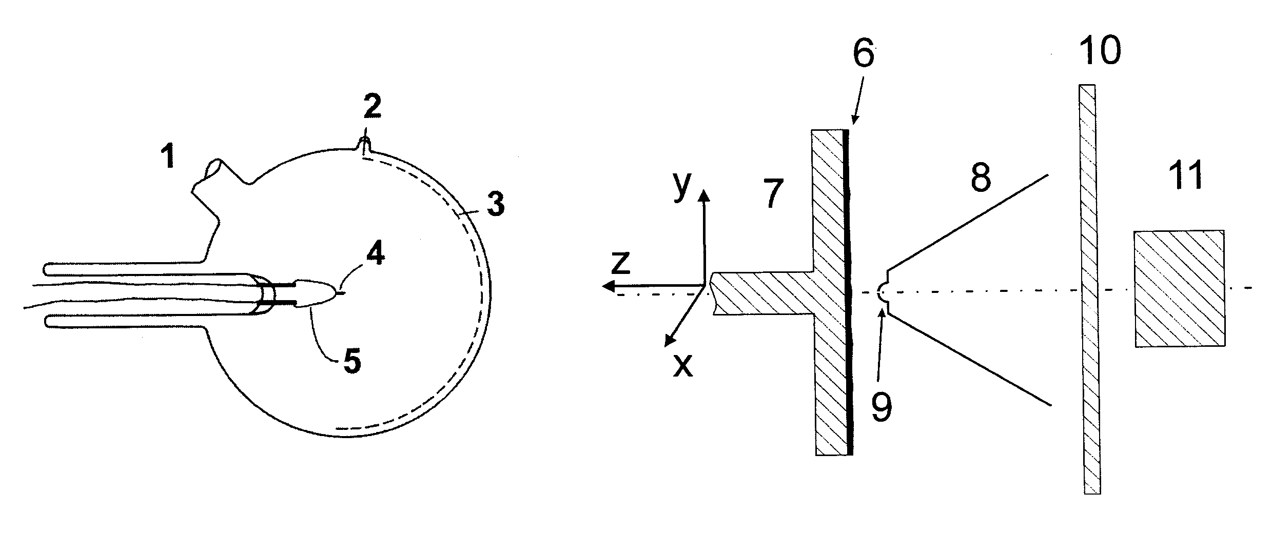
Subject of the invention is a field microscope for the examination of emission areas on the surface of cold flat cathodes. This is a new instrument which enables magnitude measurements of the emitted electric current originating from the individual emission spot on the surface of a cold cathode and at the same time its monitoring regarding emission current at the level of atomic resolution. The microscope according to the invention is characterised in that the examined flat cold cathode (6) at zero potential is located across the hand of the manipulating device (7) which enables XYZ shifting of the cathode within the container, where prior to the measurement an ultra high vacuum has been generated, transmitting electrons from individual emitters in the direction of the hollow metal cone (8) which is terminated on top by a shutter inside a ball-shaped cap (9) on the positive potential being by an electric field focused on a flat luminescent screen (10) featuring an equal or higher positive potential where these electrons are monitored or captured by a CCD camera (11) as an emission sample. The advantage of the microscope according to the invention is that it creates a uniform electronic field only in the very proximity of the screen which is located on top of the ball-shaped cap where the electrons are directed inside a weak electric field towards the screen. The electric field with a radial distance from the screen decreases which contributes to a favourable ratio between the emitted and screen-focused current. By moving the sample on a selected distance Z, an XY display of the distribution of the emission locations across an extensive cathode can be created. |
| Drawings: |
 |
| Category: |
Physical Sciences |
| Technology application codes: |
Physical and exact sciences, Electronics, IT and telecoms, Measurements and standards |
| Market application codes: |
Other electronics related, Industrial products |
| www: |
https://worldwide.espacenet.com/patent/search/family/039575715/publication/SI22425A?q=si22425 |
| Patent offices: |
UIL RS |

